Two machines in the MicrodeviceLaboratory.

MicroDevice Laboratory

Our Mission

The multi-user MicroDevice Laboratory (MDL) is housed within a 1,000-square feet cleanroom at Stevens Institute of Technology. It is a multiuser facility that provides cutting edge micro/nano-fabrication and characterization facilities to support the research and educational programs of the Institute. It furthermore provides hands-on research opportunities for undergraduate and graduate students.

Location and hours

Carnegie 101
Mon - Fri: 9:00 a.m. to 5:00 p.m.
Sat - Sun: 9:00 a.m. to 5:00 p.m. (Office closed)


MDL Staff

Chang-Hwan Choi (cchoi)
Chang-Hwan Choi
Director of the MDL
Jongyoun Son (json4)
Jongyoun Son
Laboratory Manager
Nima Kalantari.
Nima Kalantari
Laboratory Assistant
Maribeth Suganuma.
Maribeth Suganuma
Laboratory Assistant

Collaborating Faculty

Chang-Hwan Choi (cchoi)

Chang-Hwan Choi

Professor, Mechanical Engineering department

Eui-Hyeok Yang (eyang)

Eui-Hyeok Yang,

Professor, Department of Mechanical Engineering

Yong Shi

Yong Shi

Associate Professor, Department of Mechanical Engineering

Annie Xian Zhang (xzhang4)

Annie Xian Zhang

Associate Professor, Department of Mechanical Engineering

Stefan Strauf (sstrauf)

Stefan Strauf

Professor and Associate Chair for Graduate Studies in the Department of Physics

Yuping Huang (yhuang5)

Yuping Huang

Viola W. and Elbert C. Brinning Endowed Professor and Director of the Center for Quantum Science and Engineering

Capabilities and Equipment

Lithography
MA 6 mask aligner.

MA 6 mask aligner

  • Company: Karl Suss Microtec

  • Model: MA6/BA6

  • Operation Manuals and video

Description: The MA 6 mask aligner uses photolithography to create integrated circuits and other microelectronic devices. It transfers a pattern from a mask onto a substrate, such as a silicon wafer.


Nanoimprint lithography.

Nanoimprint lithography (NIL)

  • Company: Nanonex

  • Model: NX-1000

  • Operation Manuals and video

Description: The Nanonex NX-1000 is a advanced nanoimprint lithography (NIL) system designed for high-throughput, sub-10 nm resolution patterning. It utilizes thermal or UV-based imprinting to transfer nanoscale patterns from a mold onto substrates like silicon, glass, or polymers.


Photoresist spinner.

Photoresist spinner

Description: This machine applies a thin layer of photoresist to a substrate. The photoresist is applied in liquid form, and then the substrate is spun at high speeds to spread the liquid into a uniform film


Convection oven: Barnstead Lab-Line class 100 clean room oven.

Convection oven

  • Company: Barnstead

  • Model: Lab-Line class 100

  • Operation Manuals and video

Description: The Convection Oven is designed for precise, uniform heating in cleanroom or laboratory environments. It features forced-air convection for rapid temperature uniformity (±1–2°C) across the chamber, with a temperature range of ambient to ~300°C. The "Class 100" designation indicates compliance with cleanroom particle standards (≤100 particles/ft³), making it ideal for contamination-sensitive applications like semiconductor processing, pharmaceutical drying, or material curing.

Etching
XeF2 etcher: XACTIX Xetch e1.

XeF2 Etcher

  • Company: XACTIX(KLA)

  • Model: Xetch e1

  • Operation Manuals and video

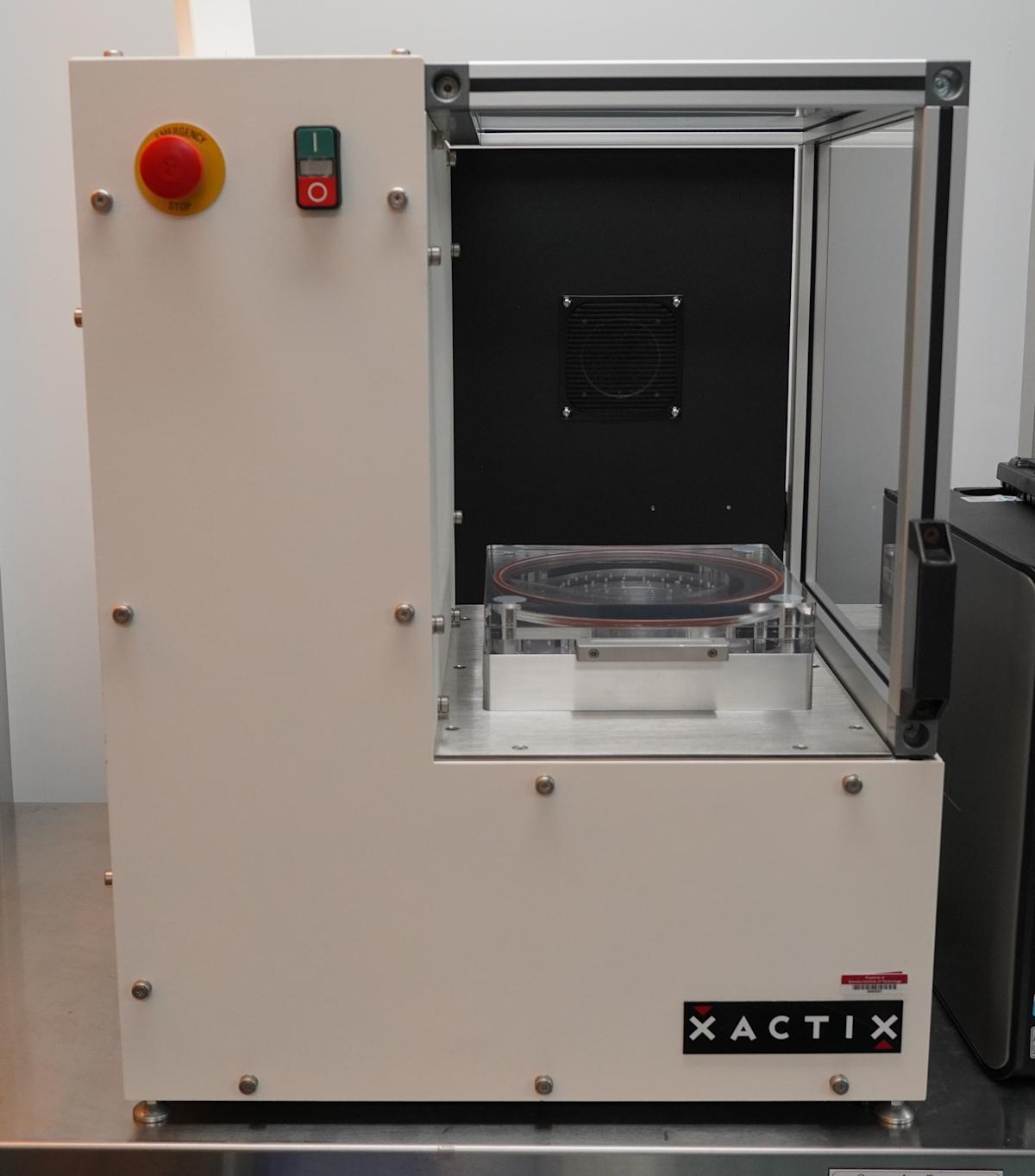
Description: XeF2 (Xenon Difluoride) is isotropic silicon etching media selective to most other materials. The system can constantly input vaporized XeF2 into reaction chamber and exhaust the etching end product at certain temperature and pressure.


Deep reactive ion etcher.

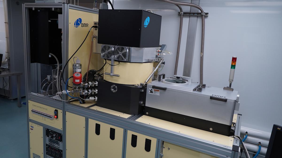
Deep reactive ion etcher (DRIE)

  • Company: BMR Technology DSE200

  • Model: DSE200

  • Operation Manuals and video

Description: This is a semiconductor fabrication tool designed for high-aspect-ratio anisotropic etching, critical for MEMS, sensors, and advanced packaging. It supports 200mm wafers and employs the Bosch process (alternating etch/passivation cycles) to achieve etch rates of 8–12 µm/min in silicon, with aspect ratios up to 30:1.


Plasma Cleaner.

Plasma Cleaner

  • Company: Plasma Etch, Inc

  • Model: PE-50

  • Operation Manuals and video

Description: The PE-50 is a compact tabletop plasma cleaner designed for surface preparation, cleaning, and activation of materials. Manufactured by Plasma Etch, it operates using air or various process gases to generate plasma in a low-pressure chamber. The system is well-suited for removing organic contamination, enhancing surface wettability, or improving adhesion for bonding or coating applications. Its fully automated control system allows for precise process tuning, while the benchtop design makes it ideal for research labs and small-scale fabrication environments.


Inductively coupled plasma etcher (ICP) .


Inductively coupled plasma etcher (ICP)

  • Company: BMR Technology

  • Model: HiEtch ICP-etcher

  • Operation Manuals and video

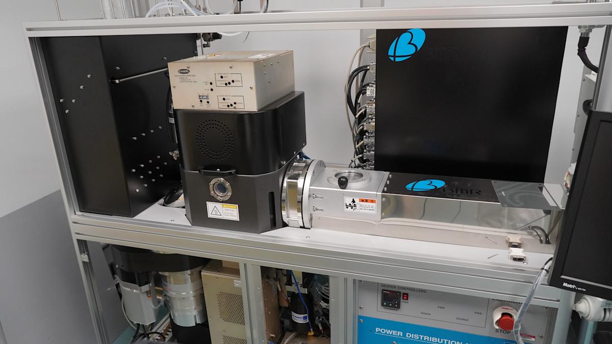
Description: The BMR HiEtch ICP-Etcher is a high-density plasma etching system designed for precision microfabrication. Using inductively coupled plasma (ICP), it enables anisotropic etching of materials like silicon, silicon dioxide, silicon nitride, and compound semiconductors (e.g., GaN, GaAs).
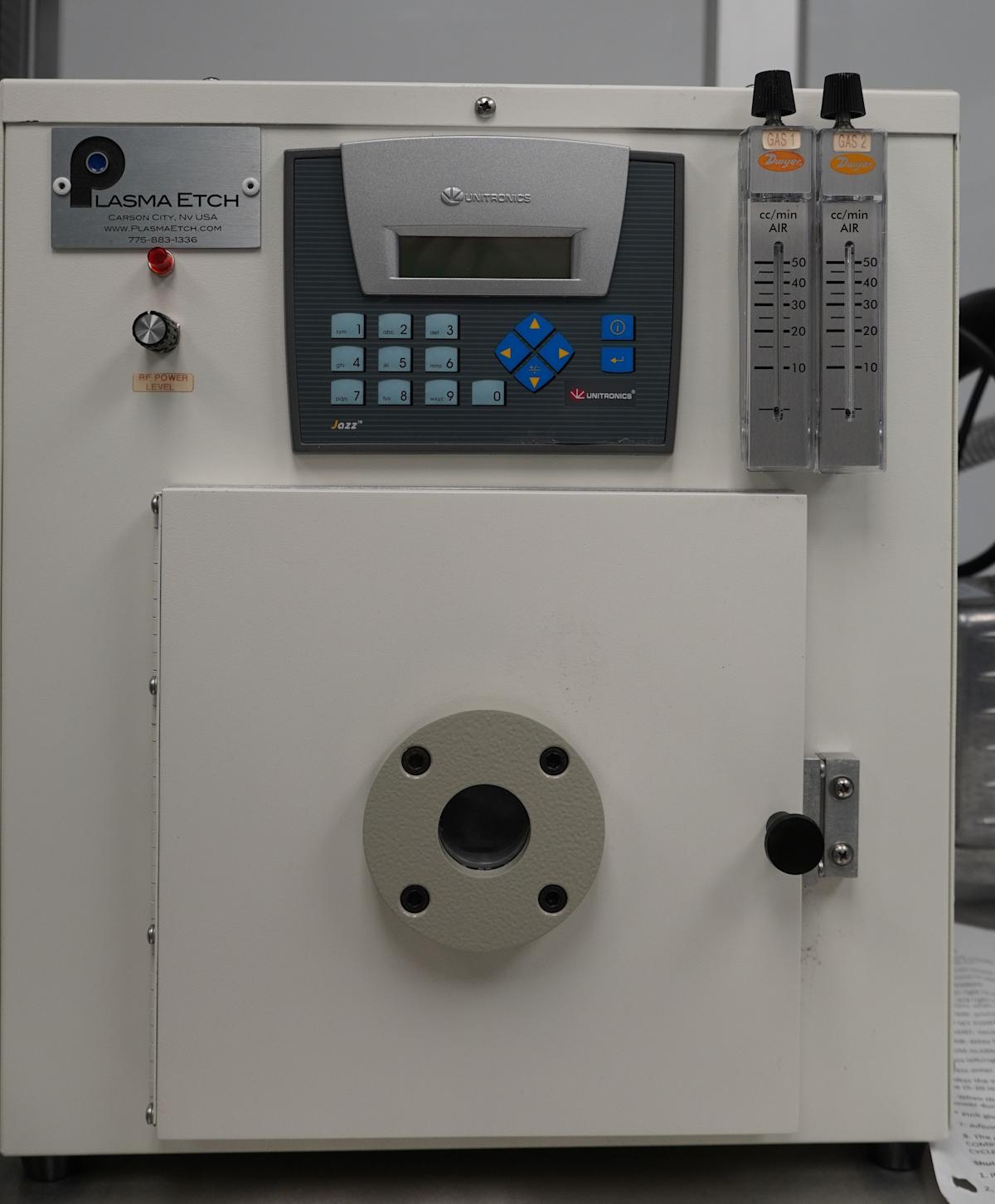
Characterization
Scanning electron microscope .

Scanning electron microscope (SEM)

Description: The Quanta FEG 450 is a high-performance scanning electron microscope equipped with a field emission gun (FEG) source, offering high-resolution imaging capabilities. It supports multiple vacuum modes—high vacuum, low vacuum, and environmental (ESEM)—allowing for the examination of a wide range of sample types, including non-conductive and hydrated specimens. With a resolution of up to 1.0 nm at 30 kV in high vacuum mode, it is suitable for detailed analysis in materials science, nanotechnology, and biological research. The system includes detectors such as secondary electron detectors (SED), backscattered electron detectors (BSED), and options for energy-dispersive X-ray spectroscopy (EDS), enhancing its analytical capabilities.


Probe station.

Probe station

Description: The Wafer Probe System is a specialized tool for stress testing and lifetime analysis of semiconductor devices under controlled electrical, thermal, and environmental conditions.


Atomic Force Microscope.

Atomic Force Microscope (AFM)

  • Company: Pacific Nanotechnology

  • Model: Nano-I2 AFM

  • Operation Manuals and video

Description: The Nano-I2 AFM by Pacific Nanotechnology is a high-precision scanning probe system designed for nanoscale surface characterization. It features an 80 µm × 80 µm XY piezoelectric scanner and an 8 µm Z-range, with closed-loop calibration sensors ensuring accurate imaging. Integrated with a 1000× video microscope and motorized zoom/focus, it enables precise sample alignment and probe positioning. The system includes a motorized XY stage with a vacuum chuck supporting up to 8” substrates, and a dedicated control unit with advanced SPM software for image analysis, lithography, and automation

Deposition
Molecular vapor deposition (MVD).

Molecular vapor deposition (MVD)

  • Company: Applied MST

  • Model: MV100

  • Operation Manuals and video

Description: The MVD system provides semi-automated deposition of organic and composite surface coatings. This system can reduce coating costs by an order of magnitude when compared with traditional techniques.


Physical vapor deposition (PVD).

Physical vapor deposition (PVD)

Description: The Explorer can accommodate substrates as large as 8 inches. The sputtering configuration accommodates DC, Pulsed DC, and RF sputtering with co-sputtering capability. Optional proprietary PEM technology is available for closed loop control transition mode and high rate reactive sputtering of metal oxides and nitrides.


Sputtering System.

Sputtering System

Description: The Pelco SC-6 is a compact, bench-top sputter coater designed for the deposition of thin metal films, typically used for sample preparation in scanning electron microscopy (SEM). It operates under low vacuum with a rotary pump and utilizes a DC magnetron sputtering source to coat non-conductive specimens with gold, palladium, or other target materials. The system provides uniform coatings and is easy to operate, making it suitable for both routine SEM prep and thin-film research. Though an older model, its core functionality remains comparable to the SC-7, with manual control of deposition parameters and robust reliability for research applications.


microFAB-3D Printer.

Micro 3D Printer

Description: The MicroFAB-3D by Microlight3D is an ultra-high-resolution 3D printing system based on two-photon polymerization (2PP), capable of fabricating complex microstructures with sub-200 nm resolution. It enables true 3D freeform printing without layering artifacts, ideal for applications in micro-optics, microfluidics, and biomedical engineering. The system supports various materials and standard substrates like glass or silicon, with stitchless printing over extended areas. Real-time imaging and precision alignment are achieved via an integrated microscope objective.

Becoming a MDL user

  • Step 1: Submit documents and review safety materials

  • Step 2: Complete safety trainings

  • Step 3: Prepare Standard Operating Procedures (SOPs)

    • Users must complete specific SOPs for their experiments

    • SOP template

  • Step 4: Walk-through and device training

    • Walk-through includes: Laboratory facilities overview, Personal Protective Equipment (PPE), safety equipment and use

    • Device training includes: lab TA demonstration of device operation

  • Step 5: Request Door access

    • Door access requests must be approved by the laboratory manger


Safety Documents


User Fees

Equipment

Hourly fee $ for Stevens Users (1 hour minimum)

Hourly fee $ for External Users 

Note

Mask aligner (MA6)

50

100

PVD

50 (excluding pumping time)

100 (excluding pumping time)

user brings crucibles/targets

DRIE

100

200

ICP etcher

100

200

XeF2 etcher

50

100

Nanoimprintor

50

100

user brings mold photoresists

Probe station

50

100

O2 Plasma

50

100

Spin coater, oven, hot plates, hood

50 (exempted if using with MA6 or etchers)

100 (exempted if using with MA6 or etchers)

user brings photoresists/developers

SEM

50

100

AFM

50

100

user brings AFM tips

Equipment training

200

300

Equipment operated by staff

100 + equipment hourly fee

100 + equipment hourly fee