MicroDevice Laboratory
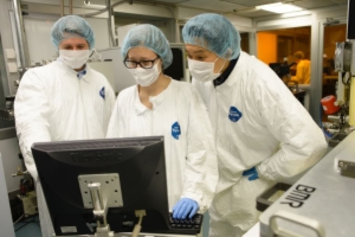
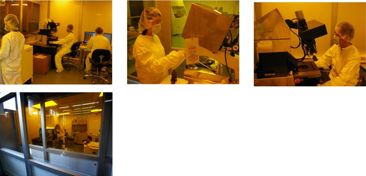
The multi-user MicroDevice Laboratory (MDL) is housed within an 800 square feet cleanroom at Stevens Institute of Technology.
Mission
The MicroDevice Laboratory (MDL) is an Institute multiuser facility whose mission is to provide cutting edge nanofabrication and characterization facilities to support the research and educational programs of then Institute. It furthermore provides hands-on research opportunities for undergraduate and graduate students.
Lab Director
Lab Staff
Dr. Kyungnam Kang (2013-current)
Postdoctoral Scholar
Ph.D. from Louisiana State University
Research: 2D materials
MicroDevice Lab Capabilities
Lithography
Mask aligner, Spin coater, Nanoimprintor, Bake ovens, Wet bench, Microscope
Device Testing
Probe station, SEM, Microscope
Etch & Deposition
DRIE, ICP, XeF2 etcher, Wet etch bench, PVD, Thermal evaporator, MVD
Facility Overview
The multi-user MicroDevice Laboratory (MDL) is housed within an 800 square feet clean room at Stevens Institute of Technology.
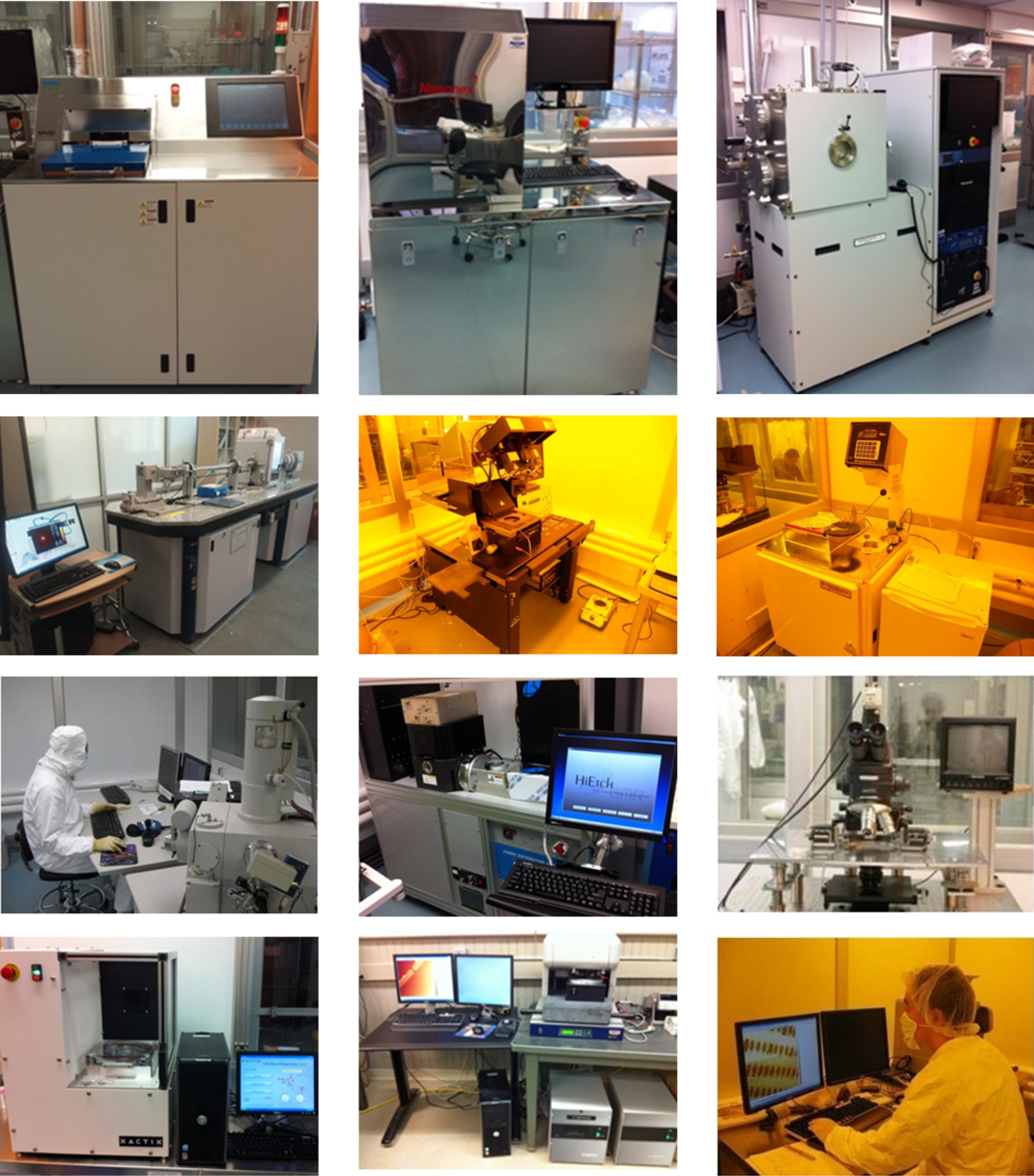
Equipment
The following pieces of equipment will be available within the facility:
A complete lithography system including Mask Aligner (Karl Suss MA6), Nanoimprintor (Nanonex), Spin Coater/Drier (Headway Research), Solvent Bench (Clean Air Products), Wet Etch Bench (Clean Air Products), Laminar Hood, Hotplate System (Alpha Multiservices), Ovens (Alpha Multiservices), and Surface treatment (O2 plasma) are available.
For characterization, Environmental Scanning Electron Microscope (SEM, FEI) is also available.
For deposition, Physical Vapor Deposition (PVD, Denton Vacuum), Thermal Evaporator (Ladd Research), Sputter Coater (Pelco), and Molecular Vapor Deposition (Applied MST) are installed. In addition, Deep Reactive Ion Etcher (DRIE, BMRTek), XeF2 Etcher (Xactix), and Inductively Coupled Plasma Etcher (ICP, BMRTek) are available along with other testing equipment such as Microscope (Nikon) and Probe Station (Signatone).
Lithography
Hot plate
Convection oven: Barnstead Lab-Line class 100 clean room oven
Spin coater: Headway Research PWM32-PS-R790
Mask aligner: Karl Suss Microtec MA6/BA6
Wet bench: Clean Air Products
Nanoimprintor: Nanonex NX-1000
Wet Etching
Wet bench: Clean Air Products
Dry Etching
XeF2 etcher: XACTIX Xetch e1
Deep reactive ion etcher (DRIE): BMR Technology DSE200
Deposition
Thermal evaporator: LADD Research filament evaporator
Physical vapor deposition (PVD): Denton Vacuum Explorer 14
Molecular vapor deposition (MVD): Applied MST
Deep Silicon Etcher
Inductively coupled plasma etcher (ICP): BMR Technology HiEtch ICP-etcher module
Characterization
Microscope
Scanning electron microscope (SEM): Quanta FEG 450 (High Vac, Low Vac, ESEM modes)
Probe station: Semiprobe Semiconductor characterization system: Keithley 4200
MDL Equipment Overview
Safety
The MDL management has implemented all reasonable measures to ensure that this cleanroom provides a safe and clean working environment. It is the responsibility of all users, guests and staff to act in a professional, courteous, and safe manner at all times while in the facility. Users violating the operating and safety rules of the facility or endangering the safety of them or other users will be denied further access to the laboratory at the sole discretion of the management.
Manuals
All manuals are available from the network drive \\storage02\medist$\MDL Manuals.
Hit Windows+R
Type \\storage02\medist$
Login using your campus Domain credential
CAMPUS\YOURUSERNAME
YOUR PASSWORD
MVD from Applied Microstructures
PVD from Denton Vacuum
XeF Etcher from Xactix
Nanoimprintor from Nanonex
SEM from FEI
DRIE and ICP from BMRTek
People
Name | Research Topic |
|---|---|
Abdus Salam Sarkar | 2D materials |
Chao Sui | Tissue/organ-on-chip and immunotherapy |
Elham Easy | Study of microstructure of additive manufacturing devices |
Greg Hader | Nano-sheet resonators |
Hearsh Hoshing | |
Hibal Ahmad | Thermal conductivity |
Javid Akhavan Taheri Boroujeni | 3D printing |
Jeric Hernandez | 2D material for thermoelectric measurement |
Jongyoun Son | ME Lab manager |
Ke Xu | |
Licheng Xiao | |
Kyungnam Kang | MDL manager |
Mengqi Fang | 2D material growth |
Na Liu | 2D material optical property measurement |
Seyed S Mohajerani | |
Seyed Mohammad Hosseini | 3D printing |
Shuai Yu | pHEMA hydrogel fabrication |
Siwei Chen | MTJ fabrication |
Yazhou Zhou | |
Yingtao Wang | Graphene device |
Youmna Mahmoud | 3D printing |
Yunong Tang | 2D materials fabrication |
Zheqi Li | Carbon nanotubes |
Zitao Tang | Graphene ring |
User Fees
Equipment | Hourly fee $ for Stevens Users (1 hour minimum) | Hourly fee $ for External Users | Note |
|---|---|---|---|
Mask aligner (MA6) | 50 | 100 | |
PVD | 50 (excluding pumping time) | 100 (excluding pumping time) | user brings crucibles/targets |
DRIE | 100 | 200 | |
ICP etcher | 100 | 200 | |
XeF2 etcher | 50 | 100 | |
Nanoimprintor | 50 | 100 | user brings mold photoresists |
Probe station | 50 | 100 | |
O2 Plasma | 50 | 100 | |
Spin coater, oven, hot plates, hood | 50 (exempted if using with MA6 or etchers) | 100 (exempted if using with MA6 or etchers) | user brings photoresists/developers |
SEM | 50 | 100 | |
AFM | 50 | 100 | user brings AFM tips |
Equipment training | 200 | 300 | |
Equipment operated by staff | 100 + equipment hourly fee | 100 + equipment hourly fee |