Nature Inspired Surface Engineering (NISE) Laboratory
About
The research of our group focuses on the fundamental understanding of interfacial phenomena inspired by nature and the development of scalable manufacturing techniques that can allow the scientific studies of mechanics and the broad applications of the engineered surfaces, ultimately targeted for multifunctional/adaptable surfaces, devices, and systems for multiscale civil/military/energy applications. Some of the research highlights include:
Nanopatterning/Nanofabrication/Nanomanufacturing
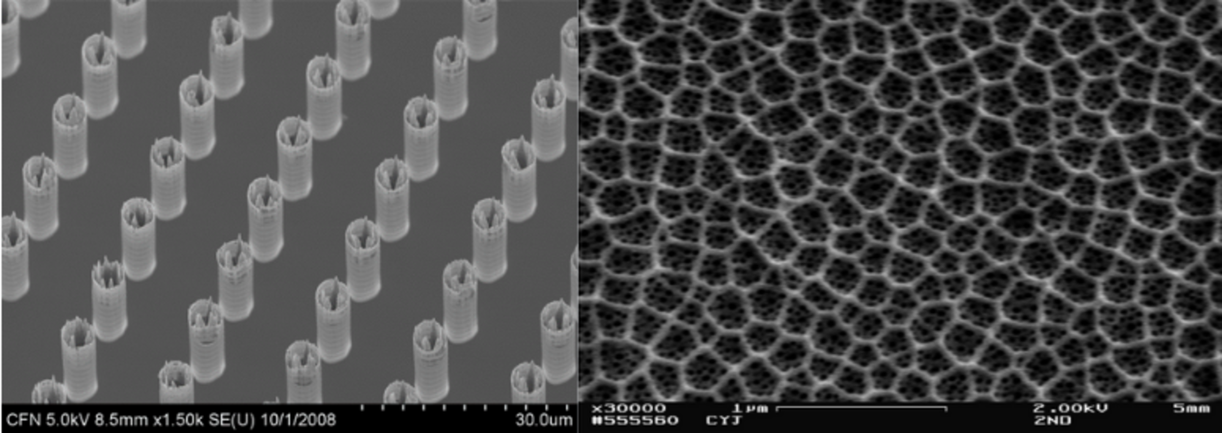
As scientific quests and engineering applications reach down to a nanometer scale, there is a strong need to fabricate three-dimensional (3D) nanostructures with precise controllability of their pattern, size, and shape over relatively large area of various types of substrate materials at low cost at high rate. One of major research achievements is in the innovation of nanomanufacturing systems and technologies, especially for large-area 3D nanopatterning and nanostructure fabrication. For full wafer-scale (and beyond), high-rate and low-cost nanolithography techniques capable of precise control of the three-dimensionality of nanostructures, tunable interference lithography systems and processes have been developed by our group. One of the systems has been issued for an US patent and recognized by the New Jersey Inventors Hall of Fame Award.
Using the well-regulated large-area periodic nanostructures as physical templates, simple pattern transfer methods for various types of thin films and nanostructures (e.g., metals and graphene) to different substrate materials including transparent and flexible substrates (e.g., glass, PDMS, and PMMA) have also been developed, which would be of great significance in many applications such as microfluidics, sensors, and wearable electronics. The nanostructured templates have also enabled site-specific layer-by-layer self-assembly of nanomaterials (e.g., nanowires, nanofibers, and nanochannels) with controlled material compositions, anisotropy, and hierarchy via physical/chemical vapor depositions as well as simple atmospheric evaporative processes. Such composite nanostructures will significantly enhance our capability to realize future smart materials and advanced systems such as high-efficiency energy harvesting materials, nanoelectronics, nanophotonics, optical/magnetic devices and sensors.
As opposed to conventional stencil lithography techniques using “hard” masks, a new “soft” stencil lithography technique has also been developed using the lithographically patterned photoresist (polymer) films as free-standing flexible membranes. Used as free-standing soft appliqué, the nanotextured flexible membrane has enabled the nanopatterning of non-planar and curved surfaces such as cylinders, spheres, trenches. Exploiting self-masking effects in oxygen plasma etching processes, a simple maskless fabrication process for high-aspect-ratio polymer nanowires has also been developed. Novel 3D anodizing techniques have also been developed, for the first time, capable of hybrid and hierarchical nanostructuring of metallic substrates. Anodization has widely been used to produce self-ordered nanostructures over a large surface area of various metallic substrates. However, the current anodizing technology normally forms only 2D planar porous structures, which seriously limit the efficacy and applicability of metallic nanostructures in many civil/military applications.
The 3D anodizing processes developed in our group have opened up a new way to realize 3D hybrid and hierarchical nanostructures via simple, convenient, and scalable electrochemical etching processes, which will significantly advance the broader applications of metallic nanostructures with immediate impacts to manufacturing industries. A highly durable oil-impregnated nanoporous surfaces of anodized metals, including aluminum and stainless steel, have also been developed via a solvent exchange method. Recently, our group has also studied the surface engineering in 3D printing.
Nanoscale Interfacial Phenomena
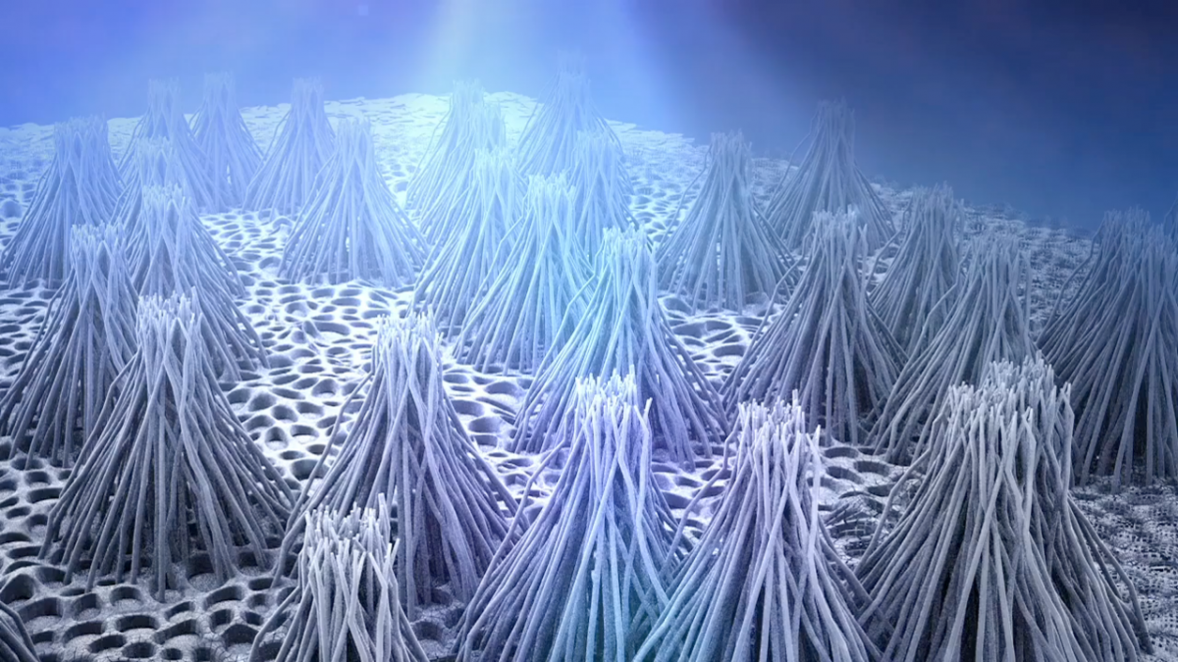
Inspired by nature, where plants, insects, and marine animals use 3D micro/nano-textured surfaces with tailored surface wettability and mechanical pliability in their components (e.g., leaves, wings, eyes, legs, and skins) for multipurpose, such as self-cleaning, low-friction, anti-fouling, anti-icing, and anti-reflection, with great energy efficiency.
Another significant scientific contribution that our group has made is in surface/interfacial science and phenomena such as wetting, friction, adhesion, and energy transfer. In particular, enabled by the large-area 3D nanopatterning systems and techniques developed in our group as described above, new fundamental understanding of novel interfacial phenomena at the nanoscale, which were unexplored previously due to the lack of experimental precision, has been established, including superhydrophobicity, contact angle hysteresis, tunable wettability of polymers, hydrodynamic slip and friction, phase-chase heat transfer processes such as evaporation, condensation, boiling, and icing, radiative energy transfer, corrosion, and microbiological cell adhesions.
One of the highlights in this area is that new physical insight on adhesion and friction of liquid drops (e.g., contact angle hysteresis) has been revealed, which is of great importance in numerous applications such as coating/spraying, microfluidics, thermal/energy systems, and biotechnology. Traditionally, it had been believed that the interfacial contact area is a key parameter to determine the adhesion and friction properties of droplets. However, our work has discovered that the dynamics of a three-phase contact line is a more direct factor to govern the adhesion and friction properties than the kinetic effect of the area. Such new discovery has further enabled a better understanding and control of broader interfacial phenomena such as tunable wettability in redox processes of conjugated (conducting) polymers and pH-dependent layer-by-layer coatings, kinetics and dynamics in mass/energy transfer processes of droplets/bubbles such as evaporation, fogging/condensation, boiling, and frosting/icing.
Another scientific breakthrough is the new understanding of wall slip flows and its engineering application to hydrodynamic friction reduction. Conventionally, a no-slip boundary condition at a solid wall had been adopted in most viscous flows, predicting the macroscale hydrodynamic behaviors very well. However, it has been discovered that the no-slip boundary condition should break down in micro and nanoscales, significantly influenced by surface roughness and wettability. Moreover, it has been shown that slip can be regulated by engineering the surface micro/nano-textures, increasing linearly with pattern periodicity and exponentially with air fraction in case of superhydrophobic surfaces. Our group has also demonstrated that such a giant slip can reduce hydrodynamic friction significantly, not only in laminar flow but also in high Reynolds number turbulent flow, which will result in great energy saving and energy conversion efficiency in many fluid engineering systems. It has also been shown that such slippery superhydrophobic surfaces prevent surfaces from corrosion and biofouling, having truly energy-efficient, multifunctional and broad applicability.
Based on the achievements and advances outlined above, the ultimate goal of on-going and future research in our group is to develop more scalable, environmentally-benign, and energy-efficient nanomanufacturing technologies and systems that can be applied to a wider range of material types. More fundamental studies and new applications of the nanoengineered surfaces/materials with tailored physical/mechanical/chemical/biological properties will be applied to broader areas, especially to address society’s most pressing global problems such as environment, energy, food, health, and water security.
Equipment
Choi’s laboratory is equipped with the major equipment required for metal 3D printing, surface patterning, treatment, characterization, and materials property measurement.
The metal 3D printer includes LENS 500 (OPTOMEC, Inc.). The LENS 500 system allows the rapid manufacturing and repair of metal components in state-of-the-art materials such as stainless steel, aluminum, titanium, and Inconel. The laser metal deposition systems use energy from a high-power fiber laser to build up structures one layer at a time directly from metal powders, alloys, ceramics or composites. The two powder feeders allow gradient materials to be made – every layer can have a different chemistry. This enables new materials to be made and analyzed with extraordinary speed. The laser metal deposition system can be used throughout the entire product lifecycle for applications ranging from rapid alloy development and functional prototyping to rapid manufacturing or repair. The LENS 500 system provides full atmosphere control, 5 axis motion, and full CNC machining as well.
The major equipment for the surface patterning includes two laser interference lithography systems. Two laser sources are available for the systems, respectively, including a HeCd laser (Kimmon Electric IK3501R-G, 50mW and 30 cm coherence length at 325 nm) and an Ar ion laser (Coherent Sabre 7, 1.7W and 1 m coherence length at 351.1 nm). They are integrated with a laser power supply (Kimmon Electric KR1801C), power meters (Newport 1918-C and 818P-001-12), 3-axis spatial filters (Newport 900), objective lenses (Newport U-27X; Thorlabs LMU-39X-NUV), pinholes (Newport 910PH-5), 6” mirrors (Melles Griot 02WBK335/028), and rotational stages (Melles Griot 07TRS001). The systems are operated in yellow lights, housed in a modular cleanroom (Class 10,000, 8’X12’X8’, Terra Universal). The custom-made laser interference lithography systems are capable of large-area nano-patterning (4-in. wafer level) with superior pattern control (well-ordered line, dot, and pit patterns down 100 nm in periodicity). Another equipment for nanoscale patterning is the electrochemical etching system, including include power supply (TDK-Lambda GEN 300-17), jacketed beaker (Chemglass CG-1103), hot plate/stirrer (VWR 12365-382), refrigerated bath (VWR 1157P), pure water container (Malgene 8-0400-08), and ductless fume hood (Sentry Air Systems SS-350-DCH). The custom-designed electrochemical etching system is capable of creating uniform nano-pore structures (50-500 nm in inter-pore distance) over a large substrate area (up to 4”X4”) with good control of electrolyte acidities, voltages, temperatures, and durations.
The equipment for the surface treatment and characterization includes molecular vapor deposition systems (MVD 100E, Applied Microstructures), a plasma cleaner (Harrick Plasma PDC-011), an ultrasonic cleaner (Branson 2510), a small angle X-ray scattering (SAXS) instrument (NANOSTAR-U, Bruker AXS), a digital microscope (Hirox KH300LCD), an advanced goniometer/tensiometer (Rame Hart Model 500), a CCD camera (Sony DFK 31BF), and custom-made environmental chambers capable of controlling chamber pressure, temperature, and humidity.
The equipment for the materials property measurement includes an inverted microscope (Nikon Ti-S), a laser confocal displacement meter (Keyence LT-9010M & LT-9510), and a programmable syringe pump (Harvard Apparatus, PHD Ultra 70-3007), a digital multimeter (Agilent 34401A), a source meter (Keithley 6487), and a potentiostat/galvanostat (Solartron Analytical).


